Während wir uns durch das Jahr 2026 bewegen, haben die industriellen und consumer Display-Märkte einen Punkt der technologischen Konvergenz erreicht. Während aufstrebende Plattformen wie MicroLED mit ihrer Helligkeit von 5.000 Nit und einer Lebensdauer von 100.000 Stunden Schlagzeilen machen, dreht sich die Kernentscheidung für die meisten Ingenieure und OEMs immer noch um den Kampf zwischen OLED und LCD.
Im modernen Ökosystem ist ein “Custom Display Manufacturer” nicht länger nur ein Lieferant, sondern ein strategischer Partner. Die Wahl zwischen diesen Technologien erfordert ein tiefes Verständnis nicht nur ihrer visuellen “Spezifikationen”, sondern auch ihrer physischen Schwachstellen. Vom permanenten Gespenst des OLED-Einbrennens bis zur allgegenwärtigen Gefahr von LCD-Druckschäden bietet dieser Leitfaden eine White-Paper-Analyse der Display-Physik, Fertigungsstandards und praxiserprobter Präventionsstrategien.
1. Vorwort: Die globale Display-Landschaft 2026
Während wir uns durch das Jahr 2026 bewegen, haben die industriellen und consumer Display-Märkte einen Punkt der technologischen Konvergenz erreicht. Während aufstrebende Plattformen wie MicroLED mit ihrer Helligkeit von 5.000 Nit und einer Lebensdauer von 100.000 Stunden Schlagzeilen machen, dreht sich die Kernentscheidung für die meisten Ingenieure und OEMs immer noch um den Kampf zwischen OLED und LCD.
Im modernen Ökosystem ist ein “Custom Display Manufacturer” nicht länger nur ein Lieferant, sondern ein strategischer Partner. Die Wahl zwischen diesen Technologien erfordert ein tiefes Verständnis nicht nur ihrer visuellen “Spezifikationen”, sondern auch ihrer physischen Schwachstellen. Vom permanenten Gespenst des OLED-Einbrennens bis zur allgegenwärtigen Gefahr von LCD-Druckschäden bietet dieser Leitfaden eine White-Paper-Analyse der Display-Physik, Fertigungsstandards und praxiserprobter Präventionsstrategien.
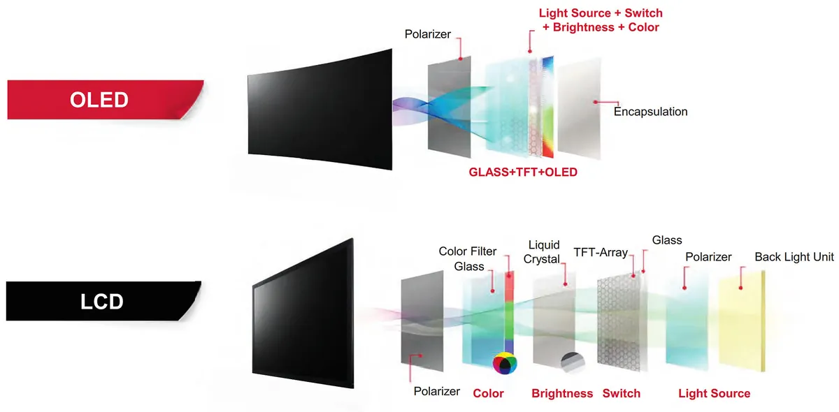
2. Technische Ontologie: Hintergrundbeleuchtung vs. selbstemittierende Modulation
Um die Leistungslücke zu definieren, muss man zunächst die grundlegende physikalische Divergenz verstehen, wie diese Bildschirme ein einzelnes Photon Licht erzeugen.
LCD (Flüssigkristallanzeige): Das Lichtventil-Paradigma
LCD ist eine nicht-emittierende Technologie. Sie ist auf eine “universelle” Lichtquelle angewiesen – die Hintergrundbeleuchtungseinheit (BLU). Moderne LCDs im Jahr 2026 verwenden hauptsächlich Mini-LED-Arrays, die Tausende von lokalen Dimmzonen bieten, um den Kontrast von OLED anzunähern, während sie die enorme Helligkeitseffizienz anorganischer LEDs beibehalten.
Das Licht durchläuft einen “Sandwich” aus Polarisatoren und einer Flüssigkristallschicht. Durch Anlegen einer Spannung an das Dünnschichttransistor-Array (TFT) rotieren die Flüssigkristallmoleküle und fungieren als Ventil, das das Licht entweder blockiert oder durch die RGB-Farbfilter passieren lässt.
OLED (Organische Leuchtdiode): Die selbstemittierende Evolution
OLED stellt einen Paradigmenwechsel dar, bei dem jedes Pixel seine eigene Lichtquelle ist. Jedes Pixel besteht aus organischen, kohlenstoffbasierten Halbleiterschichten, die leuchten, wenn Strom angelegt wird – ein Prozess, der als Elektrolumineszenz bekannt ist.
Da jedes Pixel vollständig ausgeschaltet werden kann, erreicht OLED einen sogenannten “unendlichen Kontrast” und perfekte Schwarztöne. Allerdings bleibt die “organische” Natur im Jahr 2026 ihre Achillesferse; diese Moleküle sind von Natur aus weniger stabil als die anorganischen Kristalle, die in LCDs verwendet werden, und neigen im Laufe der Zeit zu chemischem Abbau.
3. Die “Druckkrankheit”: Tiefer Einblick in LCD-Druckschäden
Für Industriedesigner und mobile OEMs ist ein Druckschaden am Bildschirm eine der kritischsten Ursachen für Feldausfälle. Im Gegensatz zu einem offensichtlichen Riss im Bildschirm äußert sich ein LCD-Druckschaden als subtile, lokalisierte Verfärbung – oft dauerhaft.
Die Physik des “Blutergusses”
Ein LCD-Panel wird durch mikroskopische Säulen, sogenannte Photo Spacer (PS), zusammengehalten. Diese Abstandshalter halten den “Zellabstand” (typischerweise 3–5 µm) aufrecht, in dem sich die Flüssigkristallflüssigkeit befindet.
Wenn übermäßige Kraft ausgeübt wird (ein Fingerdruck, ein schwerer Gegenstand auf einem geschlossenen Laptop oder unsachgemäße mechanische Montage), geschieht Folgendes:
- PS-Kollaps: Die Photo Spacer werden zerdrückt oder verschoben.
- PI-Schicht-Kratzer: Die Polyimid (PI)-Ausrichtungsschicht wird zerkratzt. Diese Schicht ist für die anfängliche Orientierung der Flüssigkristallmoleküle verantwortlich.
- Molekulare Fehlausrichtung: Sobald die PI-Schicht beschädigt ist, verlieren die Moleküle ihre “Verankerungsfähigkeit”. Sie rotieren unter Spannung nicht mehr korrekt, was zu unkontrolliertem Lichtaustritt führt.
Identifizierung von Symptomen: LCD-Fleckenschaden vs. Flüssigkeitsaustritt
Es ist entscheidend, zwischen verschiedenen LCD-Bildschirmproblemen zu unterscheiden, um die Grundursache zu identifizieren:
| Symptom | Identifikation | Physikalische Ursache |
| LCD-Fleckenschaden | Helle, weiße oder gelbliche Flecken (oft als “Mura” bezeichnet). | Lokalisierte Änderung des Zellabstands oder zerkratzte PI-Schicht durch Druck. |
| Gelbliche Höfe | Fleckige Bereiche, die hauptsächlich auf dunklen/niedriggrauen Hintergründen sichtbar sind. | Spannungsinduzierte Doppelbrechung im Polarisator oder Glasverformung. |
| Flüssigkeitsaustritt | Wachsende dunkle Kleckse oder “Tintenflecken”, die sich bei Berührung bewegen. | Bruch des Glassubstrats oder Dichtungsversagen, wodurch LC-Flüssigkeit austritt. |
| Tote/hängengebliebene Pixel | Mikroskopische, stabile helle/dunkle Punkte, die sich nicht ändern. | Elektrischer Ausfall des einzelnen Pixeltransistors. |
Technische Prävention: Industrielle Lösungen
In über 951 TP3T der Fälle sind LCD-Druckschäden irreversibel, da die innere Struktur physikalisch verformt ist. Um dies zu verhindern, muss ein führender Hersteller Folgendes implementieren:
- Hochfestes Glas: Verwendung von chemisch gehärtetem Glas (z. B. Gorilla Glass) mit einem hohen Elastizitätsmodul (> 80 GPa), um Dehnungen während der Verarbeitung und Nutzung zu widerstehen.
- Optimierte PS-Dichte: Erhöhung der Anzahl von Haupt-PS und Neben-PS pro Flächeneinheit, um Spannungen zu verteilen, wobei dies gegen die Lichtdurchlässigkeit abgewogen werden muss.
- Optisches Bonding (Marketing-Integration): Dies ist unsere effektivste Lösung. Durch das Füllen des Luftspalts zwischen dem Deckglas und dem LCD mit einem optisch klaren Klebstoff (OCA) schaffen wir eine monolithische, starre Struktur. Dies eliminiert den “Quetschfaktor” und erhöht die Widerstandsfähigkeit des Bildschirms gegen Punktdruck erheblich, wodurch das Risiko von LCD-Druckschäden praktisch ausgeschlossen wird.
4. Die Achillesferse von OLED: Organischer Zerfall und T50/T90-Metriken
Während LCDs unter mechanischem Druck leiden, leiden OLEDs unter biologischer – oder vielmehr chemischer – Alterung.
Der Einbrennmechanismus
Einbrennen ist eine dauerhafte Bildretention. Es wird durch die unterschiedliche Alterung von Subpixeln verursacht. Blaue Subpixel sind am empfindlichsten; sie haben die geringste Lichtemissionseffizienz und müssen mit höherem Strom angesteuert werden, um die Helligkeit von Rot und Grün zu erreichen.
Im Jahr 2026 hat die Industrie auf deuterierte Materialien umgestellt. Durch den Ersatz von Wasserstoffatomen in den organischen Molekülen durch Deuterium (schwerer Wasserstoff) haben Hersteller eine achtfache Steigerung der T90 (die Zeit, die ein Pixel benötigt, um auf 901 TP3T seiner anfänglichen Leuchtdichte zu fallen) erreicht.
Tandem OLED 2.0
Um Lebensdauerprobleme zu bekämpfen, verwenden High-End-Laptops und Automobildisplays im Jahr 2026 die Tandem-OLED-Architektur. Diese stapelt zwei Schichten organischen Materials, wodurch die elektrische Belastung jeder Schicht zur Erzeugung derselben Helligkeit effektiv halbiert und somit die Lebensdauer verdoppelt wird.
5. Das industrielle Diagnosehandbuch: Lösung von LCD-Bildschirmproblemen
Ein robuster QC-Prozess muss Fehler identifizieren, bevor sie den Kunden erreichen. In Gen 11-Fabriken ist die KI-gesteuerte automatisierte optische Inspektion (AOI) der Standard., Häufige Ausfallarten in der FMEA (Fehlermöglichkeits- und Einflussanalyse) Gemäß den IATF 16949-Standards müssen wir jedes potenzielle Risiko analysieren:.
V-Line Mura
: Vertikale Linien, verursacht durch Düsenverstopfung während des Fotolack-Beschichtungsprozesses. IATF 16949 standards, we must analyze every potential risk:
- V-Line Mura: Vertical lines caused by nozzle clogging during the photoresist coating process.
- ACF-Fehler: Wenn der Anpressdruck des anisotropen leitfähigen Films nicht korrekt ist, wird die elektrische Verbindung zwischen dem IC und dem Glas unterbrochen, was zu vertikalen Linienfehlern im Feld führt.
- Umgebungsbedingter Stress: Hohe Luftfeuchtigkeit kann elektrochemische Korrosion der ITO-Elektroden verursachen, was zu “Geisterbildern” oder Flimmern führt.
- Mechanisches Drehmoment: Ein zu hohes Anzugsdrehmoment der Befestigungsschrauben eines Displayrahmens kann das LCD-“Sandwich” ungleichmäßig zusammendrücken und dauerhafte Druckschäden auf dem Bildschirm verursachen.
6. Fertigungsexzellenz: Die EEAT der Displaytechnik
Autorität in der Displayfertigung wird im Reinraum aufgebaut und durch internationale Normen verifiziert.
Reinraum-ISO-Klassifizierungen
Mikroskopische Partikel sind der Feind der Ausbeute. Ein einziges Staubkorn im Array-Prozess kann einen permanenten dunklen Fleck verursachen.
| Produktionsstufe | Reinraumklasse (FED 209E) | ISO-Äquivalent | Max. Partikel (> 0,5 µm) |
| Array (Fotolithografie) | Klasse 10 | ISO 4 | 10 pro ft³ |
| Zelle (Ausrichtung/ODF) | Klasse 100 | ISO 5 | 100 pro ft³ |
| Modul (Endmontage) | Klasse 10.000 | ISO 7 | 10.000 pro ft³ |
Qualitätsstandards für spezialisierte Bereiche
- IATF 16949 (Automobil): Schreibt ein Null-Fehler-Qualitätsmanagementsystem vor. Unverzichtbar für ADAS-Displays, bei denen ein Pixelfehler ein Sicherheitsrisiko darstellen könnte.
- ISO 13485 (Medizin): Erforderlich für Diagnosemonitore. Beinhaltet strenge Rückverfolgbarkeit, sodass jedes Panel auf seine spezifische Charge Flüssigkristall zurückgeführt werden kann.
- DICOM Teil 14: Stellt die Graustufengenauigkeit sicher. Ein medizinisches LCD muss garantieren, dass ein Pixelwert von 512 genau 51,2 % heller ist als 256 – entscheidend für die Tumordetektion.
7. Anwendungsentscheidungsmatrix: Auswahlleitfaden 2026
Bei der Entscheidung zwischen OLED und LCD sollten die Umgebung und die “Gesamtbetriebskosten” (TCO) berücksichtigt werden.
Fall A: Das intelligente Cockpit (Automobil)
- Gewinner: Flexibles OLED für Ästhetik; Mini-LED-LCD für Langlebigkeit.
- Erkenntnis: 2026 bevorzugen Elektrofahrzeuge OLED für gebogene Pillar-to-Pillar-Displays, verlassen sich jedoch für kritische HUD-Einheiten (Head-Up-Display), bei denen hohe thermische Stabilität erforderlich ist, auf LCD.
Fall B: Industrielle HMI & Outdoor-Kioske
- Gewinner: LCD (Hohe Helligkeit).
- Erkenntnis: Außenumgebungen setzen Bildschirme hoher UV-Strahlung und variablem Druck aus. LCDs mit optischer Vergütung sind immun gegen Einbrennen durch statische UI-Elemente und wesentlich widerstandsfähiger gegen Druckschäden durch unvorsichtige Benutzer.
Fall C: Medizinische Bildgebung
- Gewinner: IPS-LCD.
- Erkenntnis: Stabilität übertrifft Kontrast. Radiologen benötigen Displays, deren Helligkeit über eine 8-Stunden-Schicht nicht abweicht. Medizinische IPS-LCDs mit TUV-Augenkomfort-Zertifizierung sind der Maßstab für 2026.
8. Häufig gestellte Fragen (FAQ)
1. Wie erkenne ich, ob mein Bildschirm einen “Druckschaden” oder nur Staub hat?
Reinigen Sie die Bildschirmoberfläche. Betrachten Sie einen rein weißen Hintergrund. Wenn der Fleck eine weichkantige gelbliche oder weiße “Prellung” ist, die sich beim Abwischen nicht bewegt, handelt es sich um einen LCD-Druckschaden durch inneren Druck. Staub erscheint typischerweise als scharfer, winziger dunkler Punkt.
2. Kann ein “Druckschaden auf dem Bildschirm” ohne Austausch des Panels behoben werden?
In 95 % der Fälle nein. Die inneren Schichten sind physikalisch verformt. Sie können versuchen, das Gerät für 48–72 Stunden auszuschalten, damit die Flüssigkristalle “nachfließen” können, aber dies funktioniert selten bei dauerhaftem PS-Kollaps. Ein Austausch ist die einzige industrielle Lösung.
3. Warum ist OLED teurer in der Herstellung als LCD?
OLED erfordert komplexe Vakuumbedampfungsprozesse und teure organische Materialien. Zudem liegen die Ausbeuteraten für großflächige OLED (Gen 8.6) derzeit bei etwa 80 %, während ausgereifte LCD-Linien (Gen 10.5) nahe 95 %+ erreichen.
4. Was ist “Mura” und warum tritt es häufig bei LCDs auf?
Mura ist ein japanischer Begriff für Ungleichmäßigkeit. Es umfasst LCD-Bildschirmprobleme wie Wolkenbildung oder Fleckigkeit, verursacht durch ungleichmäßige Hintergrundbeleuchtungsverteilung oder lokale Spannungen durch den Rahmen. KI-Inspektion wird verwendet, um Panels mit Mura-Level 1 auszusortieren.
5. Verhindert optische Vergütung tatsächlich “LCD-Druckschäden”?
Ja. Durch die Beseitigung des Luftspalts und die Unterstützung der gesamten Oberfläche mit einer Klebeschicht wird Punktdruck über das gesamte Panel verteilt, anstatt die internen Photo-Spacer zu zerdrücken.